|
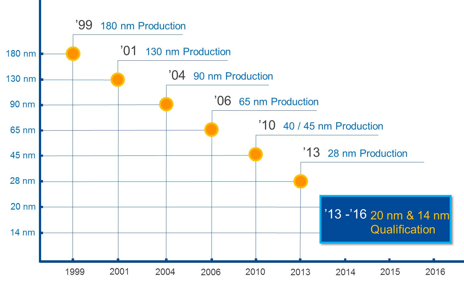
Leading the way to next generation reticle technology. As the semiconductor industry technology migrated from generation to generation, TCE provided photomask solutions that assisted customers in meeting the complex challenges of these new technologies. Now, as the industry moves toward even more advanced process technology, TCE is providing customers with the knowledge, resources, products, and solutions necessary for success at the sub 100-nanometer level. Today, TCE is one of Asian-based photomask providers continual offering nanometer process node research, development and test production. TCE and parent company Toppan have made continual investments in advanced E-beam writers, and own and operate state-of-the-art EBM6000 and EBM7500T E-beam writers. These devices will help TCE's mass production of 28 nanometer node and facilitate development of advanced photomask solutions at 14 nanometer process node and below. |
 |
|
The photomask is an essential device to be used in the manufacturing process of integrated circuits such as LSI. It is a transparent glass plate (composite quartz) on which extremely fine microcircuit patterns are etched on the light shielded film and plays a role as a master when circuits are printed on silicon wafers. The patterns on the photomask are reduced and optically transferred onto wafers to form fine patterns. Mask patterns are formed on a blank substrate based on circuit pattern data using electron beam lithography technology. The photomask is fabricated through etching, resist strip, cleaning, measurement, and inspection processes. TCE has been supporting the semiconductor industry through its manufacture of photomasks since 1997. At the same time, in order to satisfy the demand for much finer patterns on evolving LSIs, we are continuously developing phase-shifting masks and more advanced photomask products using the next generation of exposure technology. |
|
|
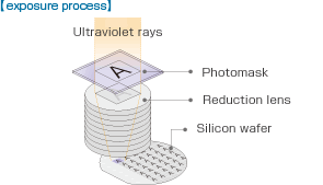
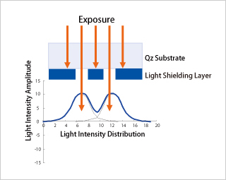
In the manufacturing process of semiconductors such as LSI, a pattern on the photomask is reduced and exposed on a silicon wafer a number of times while the stepper (i.e. reduced projection type exposure machine) shifts, transferring multiple element patterns on each wafer. |
| 1.Photomask Blanks | |
|---|---|
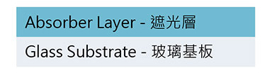 |
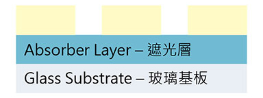
Absorber layers (chrome etc.) are deposited over the ultra fine polished high purity synthetic quartz substrate, forming a light shielding layer with a thickness of tens of nanometers. Above quartz substrate is called a photomask blanks. |
| 2.Exposure(Patterning) | |
|---|---|
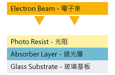 |
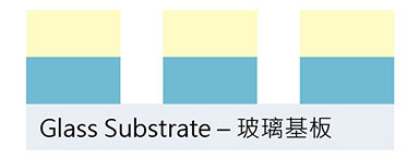
Photoresist (photosensitive resin) is uniformly coated over the surface of a photomask blanks, then a LSI circuit pattern is written by using electron beam or laser beam. |
| 3.Development | |
|---|---|
 |
The portions of resist exposed to the electron beam are removed through development process (positive tone resist). Depending on the type of resist, there are cases in which non-exposed portions of resist are removed on the contrary (negative tone resist). |
| 4.Etching | |
|---|---|
 |
The portions from which resist was removed by the development process, the absorber layer is exposed then this layer is etched through a chemical reaction by dry etching. |
| 5.Resist Removal | |
|---|---|
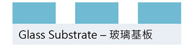 |
A photomask is completed upon removal of the resist and cleaned, and is finally shipped after passing several strict inspection processes. |
| Binary Masks | |
|---|---|
 |
Structure of binary mask is simple; it is a photomask blank covered with patterned layer of opaque material. Its transmission characteristics are either transparent or non-transparent. Binary mask is used for building a pattern in which line width being larger than the exposure wave length. |
| Phase Shift Masks | |
|---|---|
|
Phase-shifting mask (PSM) has achieved improved wafer printability with higher resolution and increased DOF (Depth of Focus), by controlling the phase shift and the transmission rate. This is a standard technology for lithography in which line width being smaller than the exposure wave length. Most well known PSM is Halftone mask (Attenuated PSM) and Levenson mask (Alternating PSM). |
|
| Half-tone Phase Shift Mask | |
|---|---|
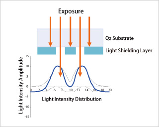 |
Half-tone mask includes chrome layer and semitransparent layer that shift the phase angle of an incoming light by 180 degree. When light passing through materials, its speed is altered, which in turn, its phase angle is shifted. This material, a semitransparent layer is called "phase shifter". Half-tone masks have achieved higher resolution, utilizing the interference of light created by a phase differences between with-phase shifter and without-phase shifter on the photomask blank. |
 |
| 2017 | SEMINAR | TITLE |
|---|---|---|
| TTF | Introduction to Toppan Technology Forum 2017 | |
| TTF | Development Trend of Product and IP with Logic NVM | |
| TTF | Introduction of Integrated Design Technology for Non-volatile Memory | |
| TTF | Reflecting on EUV mask and Lithography | |
| TTF | Challenges and Opportunities for Integrated Circuit Industry in New Formats | |
| TTF | Toppan Advanced Mask Technology | |
| TTF | Turning Strategy into Reality - A New Era in Asia for the Photomask Industry | |
| TTF | TCE Photomask Technical and Manufacturing Efforts |
| 2016 | SEMINAR | TITLE |
|---|---|---|
| TTF | Introduction to Toppan Technology Forum 2016 | |
| TTF | Reshaping Semiconductor Ecosystem | |
| TTF | RF Front-End Design Technology | |
| TTF | TCE Advanced Mask Technologies | |
| TTF | Toppan Asia-Pacific Photomask Strategy | |
| TTF | Toppan Advanced Photomask Technologies and Roadmap | |
| TTF | Concurrence and Challenge in IoT in Taiwan Semiconductor Industry | |
| TTF | EUV Mask Technology |
| 2015 | SEMINAR | TITLE |
|---|---|---|
| TTF |
Touch Free Mask Data Handling |
|
| TTF | TCE Advanced Photomask Technologies | |
| TTF | Toppan Advanced Photomask Technologies | |
| TTF | Advanced Photomask Blanks Technology | |
| TTF | EUV Mask Technology | |
| TTF | Toppan Sensor IC Development Business |
| 2014 | SEMINAR | TITLE |
|---|---|---|
| TTF | The Challenges for Mask Data Handling | |
| TTF | TCE Mask Technology and Strategy for Taiwan Customer Support | |
| TTF | Overcoming the Tribulations of 7nm patterning | |
| TTF | Optimized Solution for the Memory Layout Design | |
| TTF | Introduction to Toppan On-Chip Color Filter Technology | |
| TTF | Foundry Solution-UMC Advanced Technology |
| 2013 | SEMINAR | TITLE |
|---|---|---|
| TTF | TCE Advanced Mask Technology | |
| TTF | Toppan Mask Roadmap and Strategy for Taiwan Customer Support | |
| TTF | EUV Mask Technology | |
| TTF | Lithography Trend and Requirements for Mask Technology | |
| TTF | Design Support for IDM,Foundry and Fabless DH | |
| TTF | Overview of Toppan Technologies for Electronics Products | |
| TTF | IS Double Helix Tracking Electronic Industry? |
| 2012 | SEMINAR | TITLE |
|---|---|---|
| TTF | Data Accuracy Enhancement in TCE | |
| TTF | TCE Advanced Mask Technology | |
| TTF | Toppan Mask Roadmap and Strategy for Taiwan Customer Support | |
| TTF | EUV Mask Technology | |
| TTF | How 3D Integrated Circuits Will Change Your World | |
| TTF | Lithography Trend and Requirements for Mask Technology | |
| TTF | Design Support for IDM,Foundry and Fabless DH | |
| TTF | Toppan R&D Activities for Electronics Products | |
| TTF | Asia ICT Top4 Classic-The Co-optition among Taiwan,Japan,China and Korea |
| 2011 | SEMINAR | TITLE |
|---|---|---|
| TTF | 3S(*) Mask Data Center *3S: Speedy, Secure and Straight | |
| TTF | Advanced Inspection, Repair and Cleaning Technology | |
| TTF | Wafer Design and Process Support through Photomask Related Technology | |
| TTF | Industry Trend and Mask Development for EUV Lithography | |
| TTF | Advanced PSM and Binary Photomask Development | |
| TTF | Advanced Photomask Technology and Roadmap | |
| TTF | New Trends and Perspectives on the Integrated Design society |
| 2010 | SEMINAR | TITLE |
|---|---|---|
| TTF | Customer Oriented MMRC. | |
| TTF | New Process Set-up and Performance for Advanced Mask Technology. | |
| TTF | The Fusion of Metrology and Inspection :Challenges and Solutions | |
| TTF | Study and Improvement Approach to 193nm Radiation Damage of Attenuated Phase-Shift Mask. | |
| TTF | Next Generation Binary and Attenuated Phase-Shift Mask. | |
| TTF | Current Status of EUVL Mask Development. | |
| TTF | TCE's Overview and Roadmap. | |
| TTF | Toppan's Advanced Mask Technology and Roadmap. |
| 2009 | SEMINAR | TITLE |
|---|---|---|
| PMJ | Reduction of MRC Error Review Time through the Simplified and Classified MRC Result |
| 2008 | SEMINAR | TITLE |
|---|---|---|
| TTF | Advanced Inspection and Cleaning Technology | |
| TTF | Advanced EB and Process Technology | |
| TTF | Mask reliability issues in wafer fab | |
| TTF | CD Metrology for 32nm and Beyond | |
| TTF | Toppan’s Approach to DFM | |
| TTF | Design Support for IDM, Foundry and Fabless DH - What TDC can do for your design? | |
| TTF | Advanced reticles - where the shore of technology meets waves of cost |
| 2007 | SEMINAR | TITLE |
|---|---|---|
| TTF | Activity for Growing Haze Prevention | |
| TTF | Reliable Measurement Method for Complicated OPC Pattern | |
| TTF | Development and Evaluation of New Binary Mask Blanks for 45nm and 32nm Technologies ( 2007 PMJ Best Paper Award) | |
| TTF | Toppan’s Approach to DFM | |
| TTF | Design Support for Foundry, IDM and Fabless DH | |
| TTF | Post Structure Fulfill Using Chrome-less Phase Shift Mask | |
| TTF | IMEC lithography activities for 45nm node and beyond: mask impact | |
| TTF | BM-Toppan Joint Development Project Overview | |
| TTF | The Dresden/AMTC Role in Toppan's Global Strategy | |
| TTF | Technologies for High-end Photomasks | |
| PMJ | Application of exposure simulation system to CD control investigation at 130-nm photolithography node | |
| PMJ | Influence of Environmental Components on Haze Growth | |
| PMJ | The Effect between Absorber Profile and Wafer Print Process Window in ArF 6% Att. PSM Mask |
| 2006 | SEMINAR | TITLE |
|---|---|---|
| TTF | Study of Chromeless Mask Quartz Defect Detection Capability for 80-nm Post Structure | |
| TTF | The latest evaluation of inspection technology | |
| TTF |
The less is the more —Non-chemical cleaning technology for sub-90nm node photomask manufacturing |
|
| TTF | Migrating from 193nm to 13.5nm-Development status of EUV mask | |
| TTF |
Wherever you are, we are! — Providing Global Solutions for Photomask Supplies and Services to Our Customers |
|
| TTF | Approach to next generation-TCE advanced technology | |
| TTF | EUV Lithography at IMEC — position in our roadmap and progress on reticles | |
| TTF | 2006 BACUS Best Poster Award-Revisiting Mask Contact Hole Measurements | |
| TTF | Approaching the extreme-Toppan Global technology support | |
| TTF | DRAM Industry Trend & Strategies | |
| TTF | Maximizing Customer Benefits-Toppan's Strategy for Photomask Business | |
| BACUS | Incoming Database Verification and Management for Mask Data Preparation | |
| BACUS | Study of Chrome-less Mask Quartz Defect Detection Capability for 80nm Post Structure | |
| BACUS | The Effect between Mask Blank Flatness and Wafer Print Process Window in ArF 6% Att. PSM Mask | |
| BACUS | Non-chemical cleaning technology for sub-90nm design node photomask manufacturing | |
| PMJ | Hybrid mask (CPL-attPSM) technology for DRAM | |
| PMJ | Advanced hybrid-mask process development |
| 2005 | SEMINAR | TITLE |
|---|---|---|
| TTF | Advanced Repair Technology — Repair Craftsmanship | |
| TTF | Resolution Enhancement Technology — Approach to Next Generation Lithography | |
| TTF | Performance of New Thin Resist and Thin Cr Photomask Process | |
| TTF | A Hope in Data Desert – OASIS | |
| TTF | Advanced Mask Options: A Global Perspective | |
| TTF | The Lithography Challenges in DRAM | |
| TTF | 65nm Reticle Development Progress — Are You Ready in 65nm Production? | |
| TTF | Developing Consumer Products in Future Technology | |
| TTF | Toppan's Strategy in Photomask Business | |
| TTF | Challenges for 65nm/45nm Technology Nodes | |
| BACUS | CAR evaluation For 65nm | |
| BACUS | Real-World Impact of Inverse Lithography Technology | |
| PMJ | Application of CPL Mask for whole Chip 65nm DRAM Patterning | |
| PMJ | Effects of Mask Bias on the Mask Error Enhancement Factor (MEEF) for Low k1 Lithography | |
| PMJ | New slit scan developer system for advanced 45nm node mask making |
| 2004 | SEMINAR | TITLE |
|---|---|---|
| Photonics Asia | Improving the performance of E-beam 2nd writing in mask alignment accuracy and pattern faultless for CPLTM technology | |
| BACUS | Reduce Process Bias of Photomask Manufacturing for Next Generation Lithography | |
| SPIE | Correlating reticle pinhole defects to wafer printability for the 90nm node lithography using advanced RET | |
| PMJ | Evaluation, Reduction and Monitoring of Progressive Defect on 193nm Reticles for Low-k1 Process |
| 2003 | SEMINAR | TITLE |
|---|---|---|
| BACUS | Low k1 lithography patterning options for 90nm node | |
| BACUS | Effect of dry etching pattern profile on the chromeless phase lithography (CPL) mask | |
| BACUS | 90nm production by using AAPSM with practical image imbalance correction | |
| PMJ | Investigation of phase variation impact on CPL PSM for Low k1 imaging | |
| PMJ | Practical approach for AAPSM image imbalance correlation for Sub-100nm lithography |
| 2002 | SEMINAR | TITLE |
|---|---|---|
| PMJ | The Comparison Between Positive and Negative 50Kev E-beam CAR for 0.10um Generation | |
| PMJ | The Process of Manufacturing & Inspection of High-end (Ternary) Tritone EAPSMs Reticles for 0.13um Design Rule generation | |
| PMJ | The Comparison and Correlation of VSS Simulation Results Using Image from Different Inspection Tools |