|
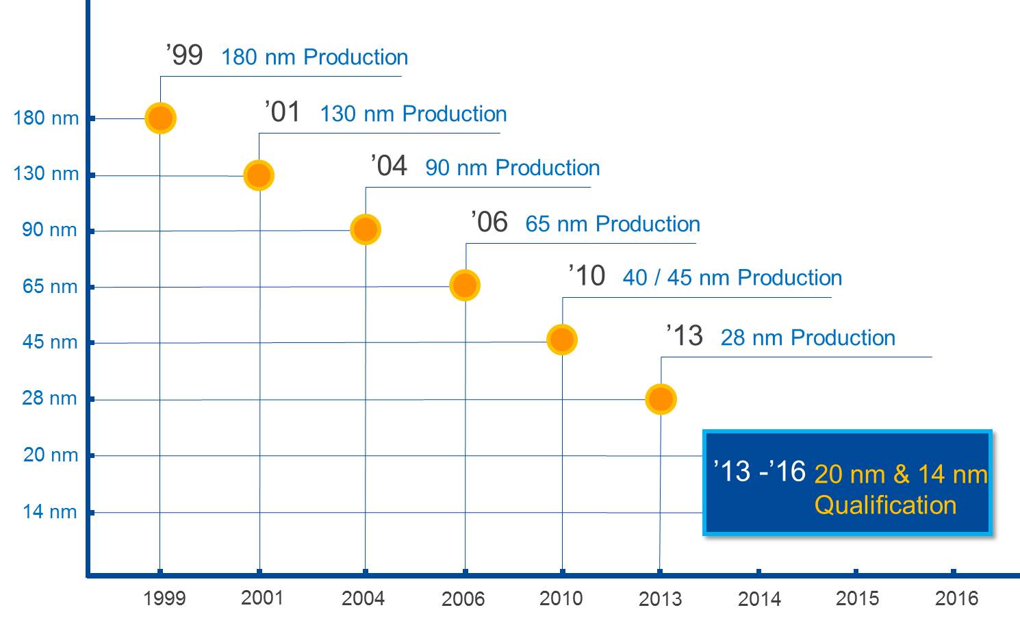
Leading the way to next generation reticle technology. 半導體產業的製程技術,隨世代持續演進,中華凸版提供的光罩解決方案,協助客戶去因應這新技術的挑戰。現在,當客戶更往先進技術邁進之時,中華凸版也在深次微米的世代,提供必需的知識、資源、產品及解決方案。 中華凸版為亞洲的光罩供應商中,持續投入先進開發製程的廠商。中華凸版及母公司-凸版印刷不斷投資電子束描繪機台,擁有先進的EBM6000及EBM7500T的電子束描繪機台,對中華凸版在28nm光罩量產及14nm以下的光罩研發助益極大。 |
 |
|
光罩是在積體電路,如LSI,的製造過程中使用的必要基本設備。它是一片透明的石英玻璃,其主要用途在於將積體電路之各種電路設計圖形轉化為晶圓製造廠大量生產所需的介面模具,並扮演著在電路設計被轉印到晶圓上之重要角色。光罩上的圖案微縮後經由曝光後反印至晶圓上。 基於藉由電子束微影技術的電路圖案,光罩圖案在使用的空白基板上形成。而光罩是通過蝕刻、光阻剝離、清洗、測量和檢驗製程。 自1997年以來, TCE一直透過製造光罩在半導體產業盡一份心力。為了滿足不斷發展的LSI為更精細的圖案的需求,我們以新一代曝光技術持續開發了相位移光罩和更先進的光罩產品。 |
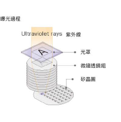 |
在半導體,如LSI,的製造過程中,在光罩的圖案被微縮並且多次在矽晶圓上曝光而步進機 ( 例如,微縮投影型曝光機 ) 移位,同時傳輸多個元件圖案到每片晶圓上。 |
| 1.光罩基板 | |
|---|---|
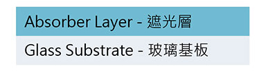 |
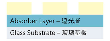
吸收層(鉻等)被沉積在超精細拋光的高純度合成石英基板,形成具有幾十納米厚度的遮光層。 上述石英基板被稱為光罩基板。 |
| 2.描畫 | |
|---|---|
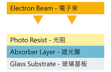 |
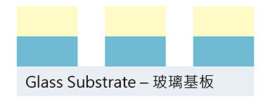
光阻(感光樹脂)是均勻塗佈在光罩的表面上,並使用電子束或雷射光束寫入LSI電路圖案。 |
| 3.顯影 | |
|---|---|
 |
光阻曝光於電子束的部分通過顯影製程去除(正光阻)。 根據光阻的種類,也有在其中未曝光部分的光阻相對被移除(負光阻)。 |
| 4.蝕刻 | |
|---|---|
 |
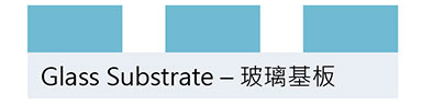
從該光阻被顯影過程除去的部分,吸收層露出光阻外並通過由乾蝕刻的化學反應完成蝕刻。 |
| 5.去除光阻 | |
|---|---|
 |
光罩在去除光阻和清洗完成,並通過一些嚴格的檢驗製程後,最後出貨。 |
| 二元光罩 | |
|---|---|
 |
二元光罩的結構簡單; 它是覆蓋有不透明材料圖案的光罩,其透光特性是透明或不透明的。基本用於線寬比曝光波長大的圖案。 然而,在32nm half-pitch以下(含)的浸潤式微影技術之應用上,二元光罩也有優於Half-tone相位移光罩的表現。 凸版和它的供應商已共同開發了新類型的二元光罩空白並具有優越的可操作性( OMOG :不透明的MoSi玻璃);他們已經成功地創造更好的二元光罩基板,包含改善的CD表現與更高的解析度。 |
| 相位移光罩 | |
|---|---|
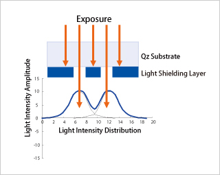
| 相位移光罩(PSM)已通過控制相位移和透光率,相位移光罩在晶圓轉印能力的改善上提供了更大的DOF(聚焦深度)。 對線寬比曝光波長小的圖案,相位移光罩是一個標準微影技術, 最著名的PSM是Attenuated PSM和Levenson Mask | |
| 半透光相位移光罩 | |
|---|---|
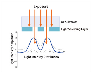 |
半透光光罩包括鉻層和可通過180度相位移穿透光的半透明層。當光穿透過材料時,其速度會被改變,且其相位角偏移。 這種半透明層的材料被稱作“相位移層”。半透光光罩是利用無相位移層與有相位移層的光的干涉而達成更高的解析。 |
 |
| 2019 | SEMINAR | TITLE |
|---|---|---|
| TTF | Introduction to Toppan Technology Forum 2019 | |
| TTF | Strategy of Toppan Photomask | |
| TTF | Introduction of development and design of sensor Ics | |
| TTF | Which Type of Photomask Is the Best from the View Point of the Wafer Lithography? | |
| TTF | Next-gen EUV Mask Materials | |
| TTF | Single Beam/Multi Beam Writer Opportunities and TCE Advanced Mask Technology for 7 nm and Beyond |
| 2018 | SEMINAR | TITLE |
|---|---|---|
| TTF | Introduction to Toppan Technology Forum 2018 | |
| TTF | EUV Mask Technology | |
| TTF | Toppan's Global Strategy of Photomask | |
| TTF | Introduction to the Most Advanced Power Management IC | |
| TTF | Toppan Advanced Mask Technology | |
| TTF | Reassuring Mask Data Handling |
| 2017 | SEMINAR | TITLE |
|---|---|---|
| TTF | Introduction to Toppan Technology Forum 2017 | |
| TTF | Development Trend of Product and IP with Logic NVM | |
| TTF | Introduction of Integrated Design Technology for Non-volatile Memory | |
| TTF | Reflecting on EUV mask and Lithography | |
| TTF | Challenges and Opportunities for Integrated Circuit Industry in New Formats | |
| TTF | Toppan Advanced Mask Technology | |
| TTF | Turning Strategy into Reality - A New Era in Asia for the Photomask Industry | |
| TTF | TCE Photomask Technical and Manufacturing Efforts |
| 2016 | SEMINAR | TITLE |
|---|---|---|
| TTF | Introduction to Toppan Technology Forum 2016 | |
| TTF | Reshaping Semiconductor Ecosystem | |
| TTF | RF Front-End Design Technology | |
| TTF | EUV Mask Technology | |
| TTF | Concurrence and Challenge in IoT in Taiwan Semiconductor Industry | |
| TTF | Toppan Advanced Photomask Technologies and Roadmap | |
| TTF | Toppan Asia-Pacific Photomask Strategy | |
| TTF | TCE Advanced Mask Technologies |
| 2015 | SEMINAR | TITLE |
|---|---|---|
| TTF | DRAM Outlook | |
| TTF | Overview of Toppan Technologies for Electronics Products ~For IoT Solution | |
| TTF | Advanced Photomask Technology and Roadmap | |
| TTF |
Touch Free Mask Data Handling |
|
| TTF | TCE Advanced Photomask Technologies | |
| TTF | Toppan Advanced Photomask Technologies | |
| TTF | Advanced Photomask Blanks Technology | |
| TTF | EUV Mask Technology | |
| TTF | Toppan Sensor IC Development Business |
| 2014 | SEMINAR | TITLE |
|---|---|---|
| TTF | The Challenges for Mask Data Handling | |
| TTF | TCE Mask Technology and Strategy for Taiwan Customer Support | |
| TTF | Overcoming the Tribulations of 7nm patterning | |
| TTF | Optimized Solution for the Memory Layout Design | |
| TTF | Introduction to Toppan On-Chip Color Filter Technology | |
| TTF | Foundry Solution-UMC Advanced Technology |
| 2013 | SEMINAR | TITLE |
|---|---|---|
| TTF |
TCE Advanced Mask Technology |
|
| TTF | Toppan Mask Roadmap and Strategy for Taiwan Customer Support | |
| TTF | EUV Mask Technology | |
| TTF | Lithography Trend and Requirements for Mask Technology | |
| TTF | Design Support for IDM,Foundry and Fabless DH | |
| TTF | Overview of Toppan Technologies for Electronics Products | |
| TTF | IS Double Helix Tracking Electronic Industry? |
| 2012 | SEMINAR | TITLE |
|---|---|---|
| TTF | Data Accuracy Enhancement in TCE | |
| TTF | TCE Advanced Mask Technology | |
| TTF | Toppan Mask Roadmap and Strategy for Taiwan Customer Support | |
| TTF | EUV Mask Technology | |
| TTF | How 3D Integrated Circuits Will Change Your World | |
| TTF | Lithography Trend and Requirements for Mask Technology | |
| TTF | Design Support for IDM,Foundry and Fabless DH | |
| TTF | Toppan R&D Activities for Electronics Products | |
| TTF | Asia ICT Top4 Classic-The Co-optition among Taiwan,Japan,China and Korea |
| 2011 | SEMINAR | TITLE |
|---|---|---|
| TTF | 3S(*) Mask Data Center *3S: Speedy, Secure and Straight | |
| TTF | Advanced Inspection, Repair and Cleaning Technology | |
| TTF | Wafer Design and Process Support through Photomask Related Technology | |
| TTF | Industry Trend and Mask Development for EUV Lithography | |
| TTF | Advanced PSM and Binary Photomask Development | |
| TTF | Advanced Photomask Technology and Roadmap | |
| TTF | New Trends and Perspectives on the Integrated Design society |
| 2010 | SEMINAR | TITLE |
|---|---|---|
| TTF | Customer Oriented MMRC. | |
| TTF | New Process Set-up and Performance for Advanced Mask Technology. | |
| TTF | The Fusion of Metrology and Inspection :Challenges and Solutions | |
| TTF | Study and Improvement Approach to 193nm Radiation Damage of Attenuated Phase-Shift Mask. | |
| TTF | Next Generation Binary and Attenuated Phase-Shift Mask. | |
| TTF | Current Status of EUVL Mask Development. | |
| TTF | TCE's Overview and Roadmap. | |
| TTF | Toppan's Advanced Mask Technology and Roadmap. |
| 2009 | SEMINAR | TITLE |
|---|---|---|
| PMJ | Reduction of MRC Error Review Time through the Simplified and Classified MRC Result |
| 2008 | SEMINAR | TITLE |
|---|---|---|
| TTF |
Advanced Inspection and Cleaning Technology |
|
| TTF | Advanced EB and Process Technology | |
| TTF | Mask reliability issues in wafer fab | |
| TTF | CD Metrology for 32nm and Beyond | |
| TTF | Toppan’s Approach to DFM | |
| TTF | Design Support for IDM, Foundry and Fabless DH - What TDC can do for your design? | |
| TTF | Advanced reticles - where the shore of technology meets waves of cost |
| 2007 | SEMINAR | TITLE |
|---|---|---|
| TTF |
Activity for Growing Haze Prevention |
|
| TTF | Reliable Measurement Method for Complicated OPC Pattern | |
| TTF | Development and Evaluation of New Binary Mask Blanks for 45nm and 32nm Technologies ( 2007 PMJ Best Paper Award) | |
| TTF | Toppan’s Approach to DFM | |
| TTF | Design Support for Foundry, IDM and Fabless DH | |
| TTF | Post Structure Fulfill Using Chrome-less Phase Shift Mask | |
| TTF | IMEC lithography activities for 45nm node and beyond: mask impact | |
| TTF | IBM-Toppan Joint Development Project Overview | |
| TTF | The Dresden/AMTC Role in Toppan's Global Strategy | |
| TTF | Technologies for High-end Photomasks | |
| PMJ | Application of exposure simulation system to CD control investigation at 130-nm photolithography node | |
| PMJ | Influence of Environmental Components on Haze Growth | |
| PMJ | The Effect between Absorber Profile and Wafer Print Process Window in ArF 6% Att. PSM Mask |
| 2006 | SEMINAR | TITLE |
|---|---|---|
| TTF | Study of Chromeless Mask Quartz Defect Detection Capability for 80-nm Post Structure | |
| TTF | The latest evaluation of inspection technology | |
| TTF |
The less is the more —Non-chemical cleaning technology for sub-90nm node photomask manufacturing |
|
| TTF | Migrating from 193nm to 13.5nm-Development status of EUV mask | |
| TTF |
Wherever you are, we are! — Providing Global Solutions for Photomask Supplies and Services to Our Customers |
|
| TTF | Approach to next generation-TCE advanced technology | |
| TTF | EUV Lithography at IMEC — position in our roadmap and progress on reticles | |
| TTF | 2006 BACUS Best Poster Award-Revisiting Mask Contact Hole Measurements | |
| TTF | Approaching the extreme-Toppan Global technology support | |
| TTF | DRAM Industry Trend & Strategies | |
| TTF | Maximizing Customer Benefits-Toppan's Strategy for Photomask Business | |
| PMJ | Advanced hybrid-mask process development | |
| PMJ | Hybrid mask (CPL-attPSM) technology for DRAM | |
| BACUS | Non-chemical cleaning technology for sub-90nm design node photomask manufacturing | |
| BACUS | The Effect between Mask Blank Flatness and Wafer Print Process Window in ArF 6% Att. PSM Mask | |
| BACUS | Study of Chrome-less Mask Quartz Defect Detection Capability for 80nm Post Structure | |
| BACUS | Incoming Database Verification and Management for Mask Data Preparation |
| 2005 | SEMINAR | TITLE |
|---|---|---|
| TTF | Advanced Repair Technology — Repair Craftsmanship | |
| TTF | Resolution Enhancement Technology — Approach to Next Generation Lithography | |
| TTF | Performance of New Thin Resist and Thin Cr Photomask Process | |
| TTF | A Hope in Data Desert – OASIS | |
| TTF | Advanced Mask Options: A Global Perspective | |
| TTF | The Lithography Challenges in DRAM | |
| TTF | 65nm Reticle Development Progress — Are You Ready in 65nm Production? | |
| TTF | Developing Consumer Products in Future Technology | |
| TTF | Toppan's Strategy in Photomask Business | |
| TTF | Challenges for 65nm/45nm Technology Nodes | |
| BACUS | CAR evaluation For 65nm | |
| BACUS | Real-World Impact of Inverse Lithography Technology | |
| PMJ | Application of CPL Mask for whole Chip 65nm DRAM Patterning | |
| PMJ | Effects of Mask Bias on the Mask Error Enhancement Factor (MEEF) for Low k1 Lithography | |
| PMJ | New slit scan developer system for advanced 45nm node mask making |
| 2004 | SEMINAR | TITLE |
|---|---|---|
| Photonics Asia | Improving the performance of E-beam 2nd writing in mask alignment accuracy and pattern faultless for CPLTM technology | |
| BACUS | Reduce Process Bias of Photomask Manufacturing for Next Generation Lithography | |
| SPIE | Correlating reticle pinhole defects to wafer printability for the 90nm node lithography using advanced RET | |
| PMJ | Evaluation, Reduction and Monitoring of Progressive Defect on 193nm Reticles for Low-k1 Process |
| 2003 | SEMINAR | TITLE |
|---|---|---|
| BACUS | Low k1 lithography patterning options for 90nm node | |
| BACUS | Effect of dry etching pattern profile on the chromeless phase lithography (CPL) mask | |
| BACUS | 90nm production by using AAPSM with practical image imbalance correction | |
| PMJ | Investigation of phase variation impact on CPL PSM for Low k1 imaging | |
| PMJ | Practical approach for AAPSM image imbalance correlation for Sub-100nm lithography |
| 2002 | SEMINAR | TITLE |
|---|---|---|
| PMJ | The Comparison Between Positive and Negative 50Kev E-beam CAR for 0.10um Generation | |
| PMJ | The Process of Manufacturing & Inspection of High-end (Ternary) Tritone EAPSMs Reticles for 0.13um Design Rule generation | |
| PMJ | The Comparison and Correlation of VSS Simulation Results Using Image from Different Inspection Tools |